
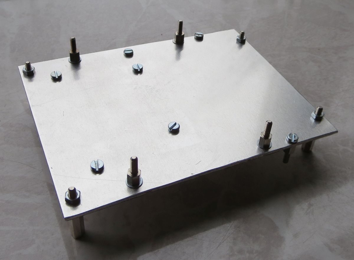
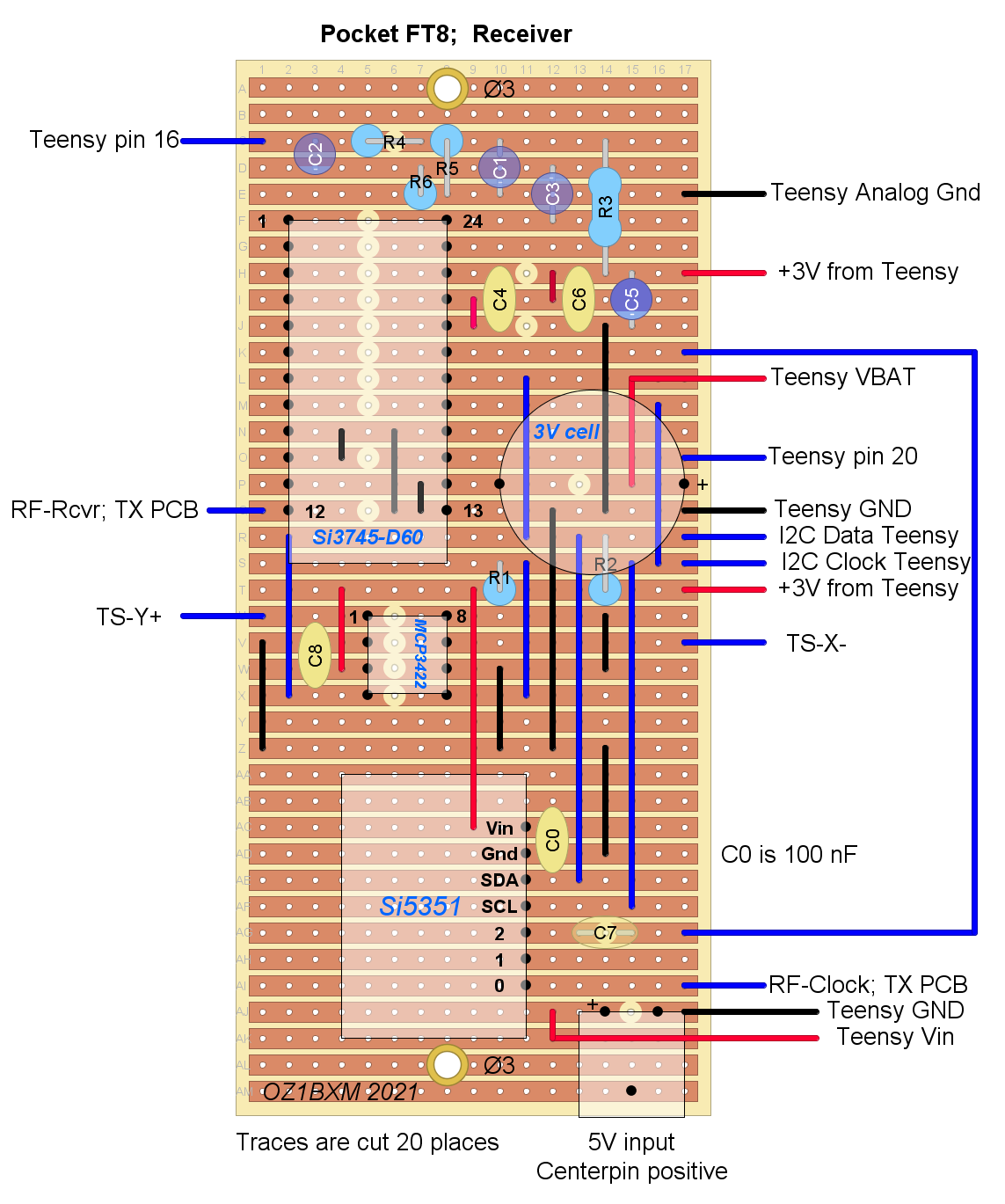
Fig. 5.Components on the receiver board. | Receiver board; components
Please refer to circuit diagram in the project manual page 3. The receiver was built on a piece of Veroboard measuring 45 mm x 100 mm. The component names are shown on this sketch which also shows a label change at Teensy pin 39.
Don't forget to cut the traces 19 different places, and drill two holes each 3 mm diameter.
Si3745 comes in a 24-pin SSOP housing (0.65 mm pitch) and is converted to 2.54 mm pitch using an SSOP-24 adapter.
My adapter is from RoarKit (sold by sheffield_nikki on ebay.com). Soldering instructions are here. Pin 10 and 11 are grounded as recommended in the data sheet page 21.
MCP3422 in a SOIC-8 house has 1.27 mm pitch and is converted to 2.54 mm pitch using an adapter with 8 pins. Soldering instructions are here.
Si5351 comes with a 2.54 mm pitch break-out board.
The decoupling capacitor C0 100 nF was added.
The round 3 V lithium cell (CR2032) is fitted last. It powers the RTC on Teensy.
|

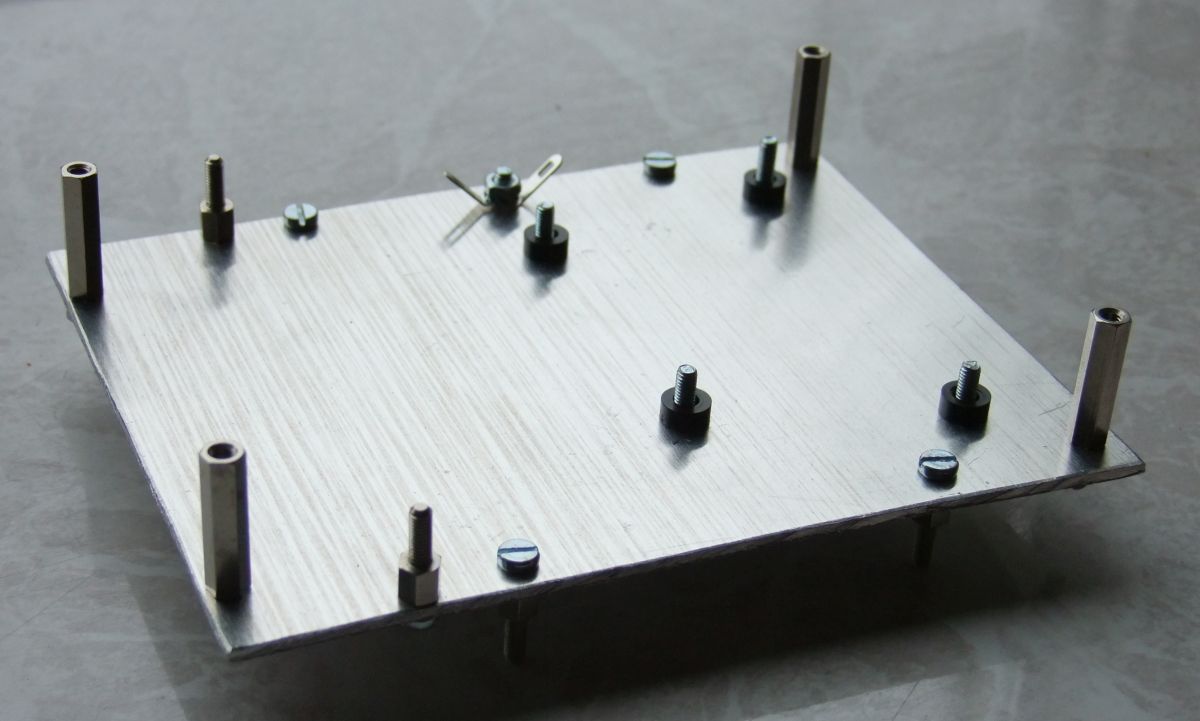
Fig 6. Receiver board without ICs and battery. | Receiver board; photo
Figure
6 shows the receiver board. The Si3745, Si5351, MCP3422,
and the battery are not fitted yet. |

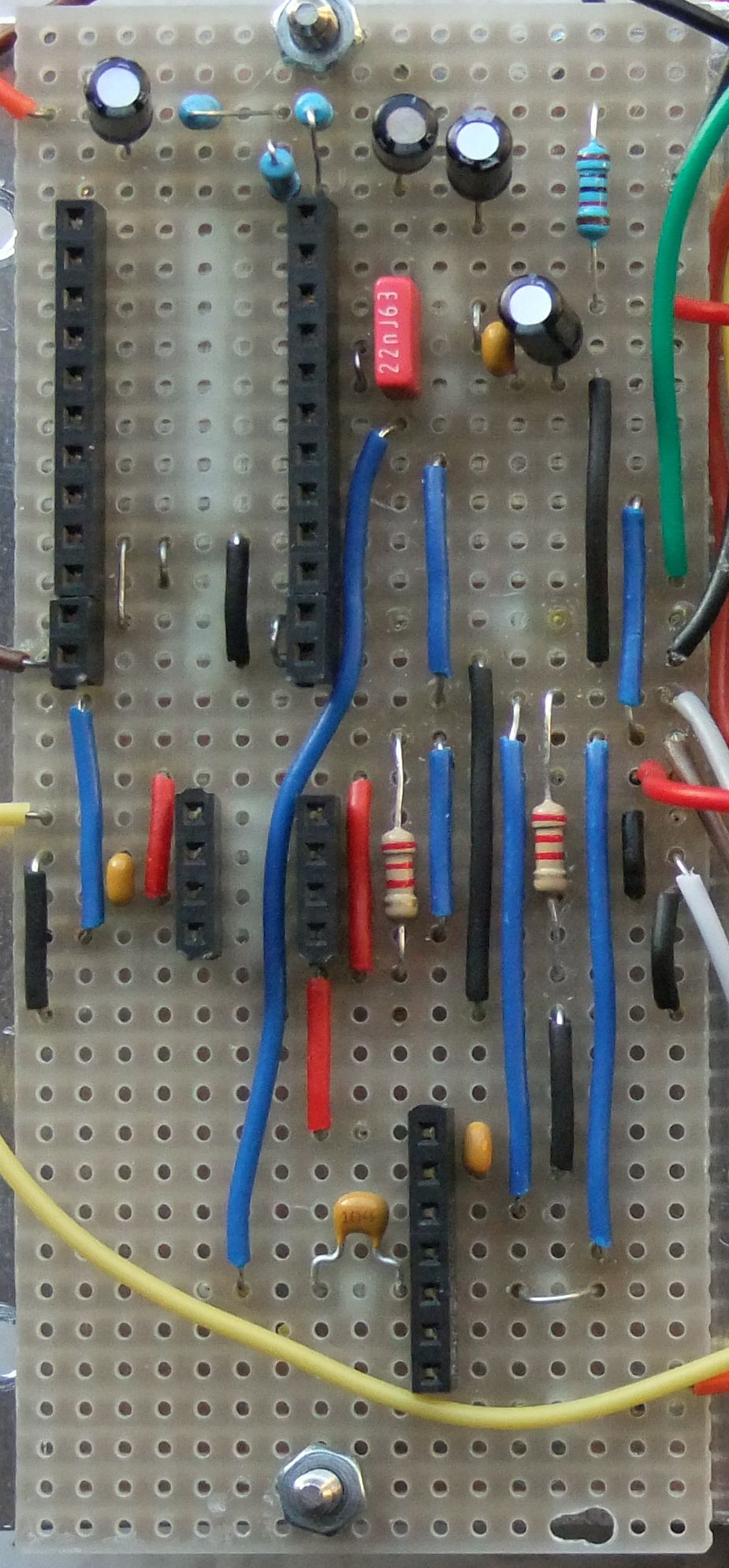
Fig. 7. Veroboard for Teensy. | Teensy 3.6 board
Teensy 3.6 is fitted on a piece of Veroboard using sockets. The Veroboard measures 68 mm x 30 mm.
Teensy 3.6 product page
Teensy 3.6 pin-out card (front side)
Teensy 3.6 pin-out card (back side)
|
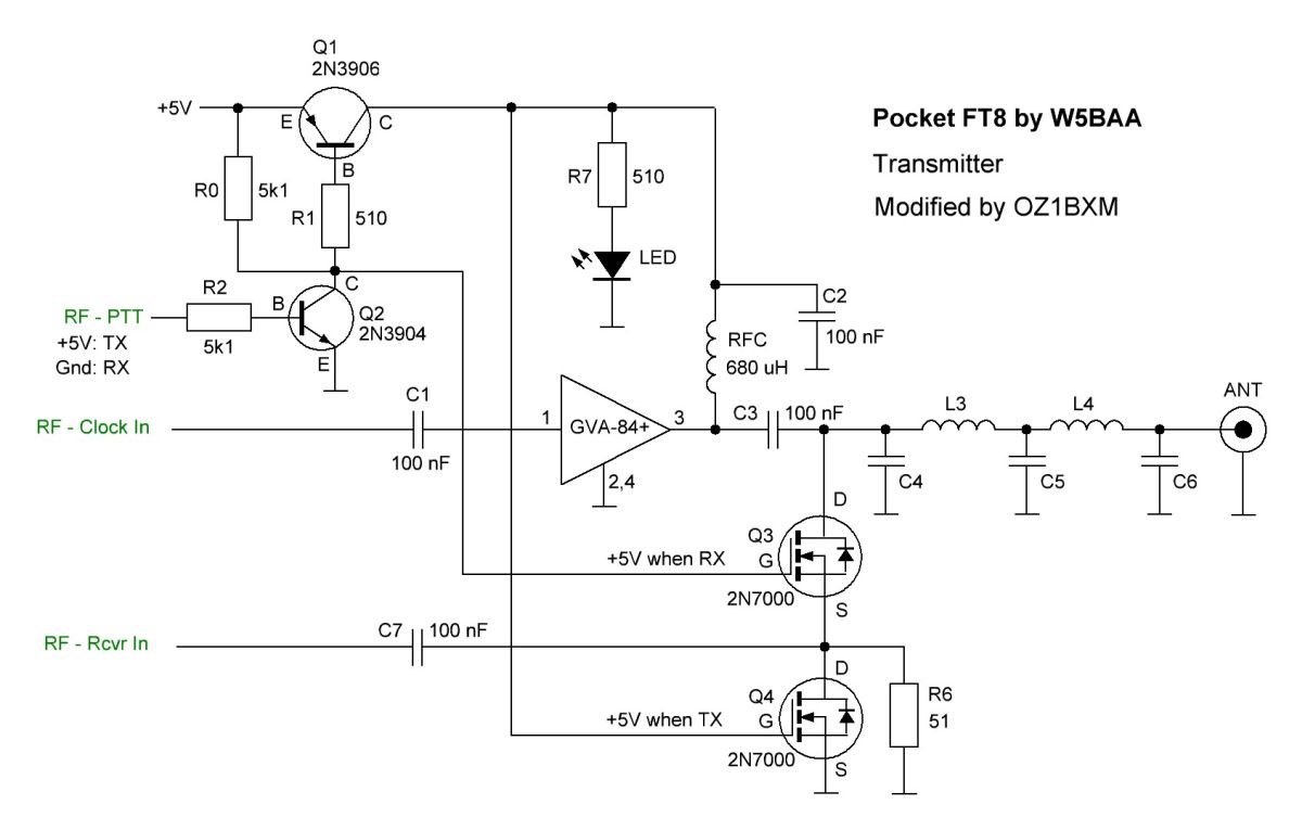
Fig. 8. Transmitter circuit diagram. | Transmitter circuit diagram
Receive:
Q3 is on; Q4 is off. The signal from the antenna
runs through the LPF and Q3 and is terminated by R6. The signal goes to the receiver via C7.
Transmit:
Q3 is
off; Q4 is on. The transmit signal from GVA-84+ flows through
the LPF to the antenna. Q3 is off and prevents the strong RF
signal from reaching the receiver. Q4 conducts and
puts "RF - Rcvr In" to ground for receiver protection.
I've modified the transmitter as shown in figure 8. Please refer to original diagram in the project manual page 4. R0
was added to allow current into Q2. R2 was added to limit the Q2
base current when RF-PTT is high. The resistor in Q3's gate was
removed (it had no function). Same destiny for the resistor in
the gate of Q4. The
input low-pass filter was removed. The low-pass
filter following GVA-84+ should be sufficient for removing
transmitter harmonics. The output transformer
T1 was removed and replaced by the application circuit from
the GVA-84+ data sheet page 4. RFC
was changed from a core-wound choke to a standard
choke. It must be the upright type (see this photo) as this type can carry more current. R7 and LED are optional. I've added the
LED to indicate when PTT is activated. Component values for 18 MHz
L3, L4: 0.5 uH. Make 10 turns 0.5 mm wire on Amidon T37-2 core. Picture of this inductor.
C4, C6: 75 pF
C5: 242 pF
|
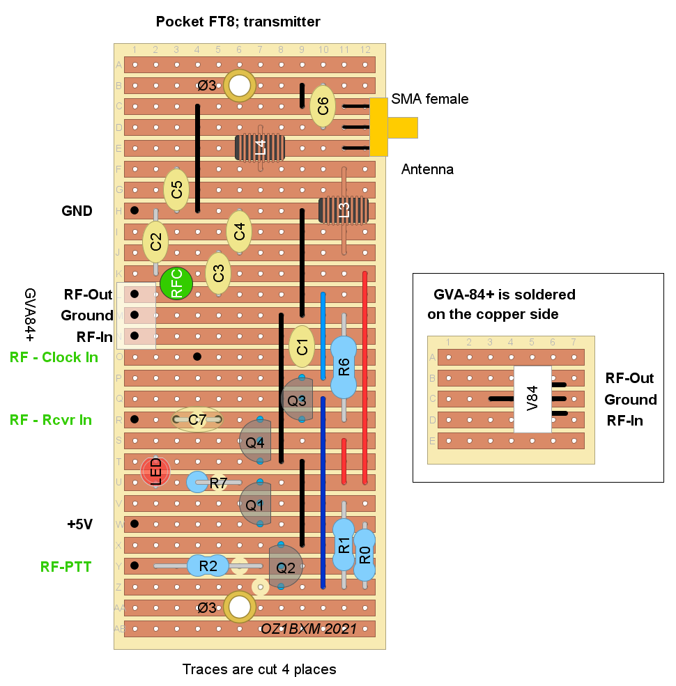
Fig. 9. Component placement, transmitter. | Transmitter board lay-out
The transmitter is buildt on a piece of Veroboard measuring 74 mm x 30 mm (figure 9).
|
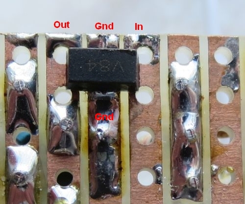
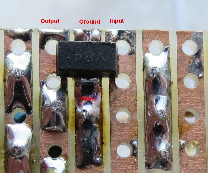
Fig. 10. Soldering GVA-84+ on the copper side. | GVA-84+
The amplifier
GVA-84+ is a surface mount component. It is placed on the
copper side of the board and soldered 4 places.
|
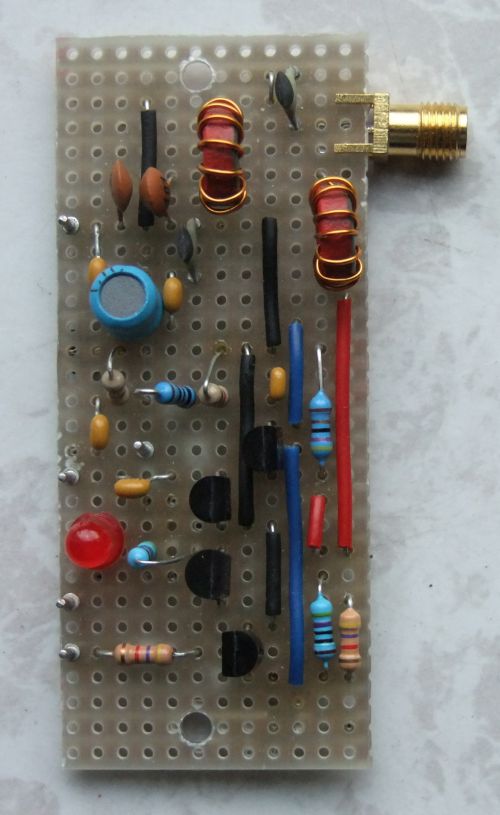
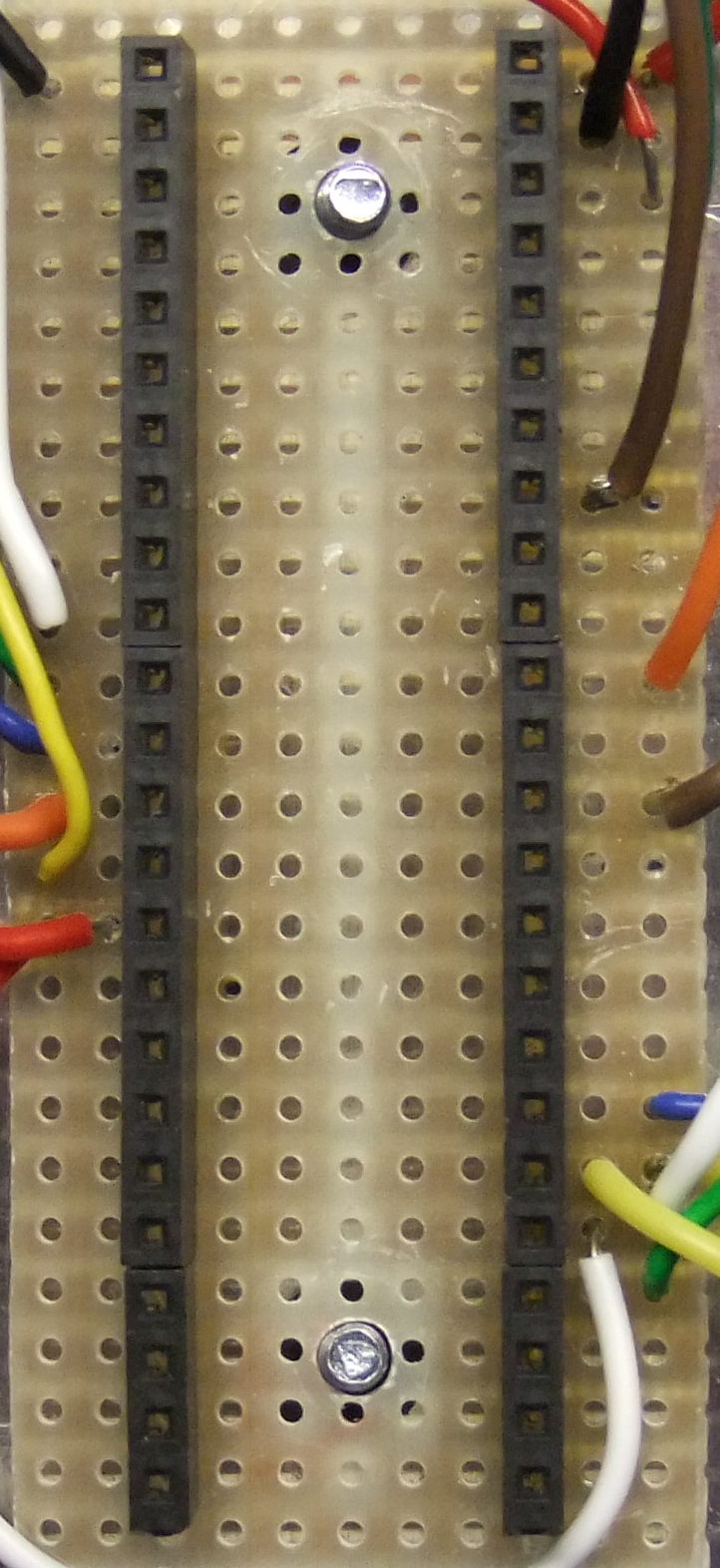
Fig. 11. Transmitter board. | Transmitter board
RF
output from the transmitter was measured
using a low-price meter from China. The output
was 50 mW at 18 MHz.
|
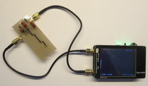
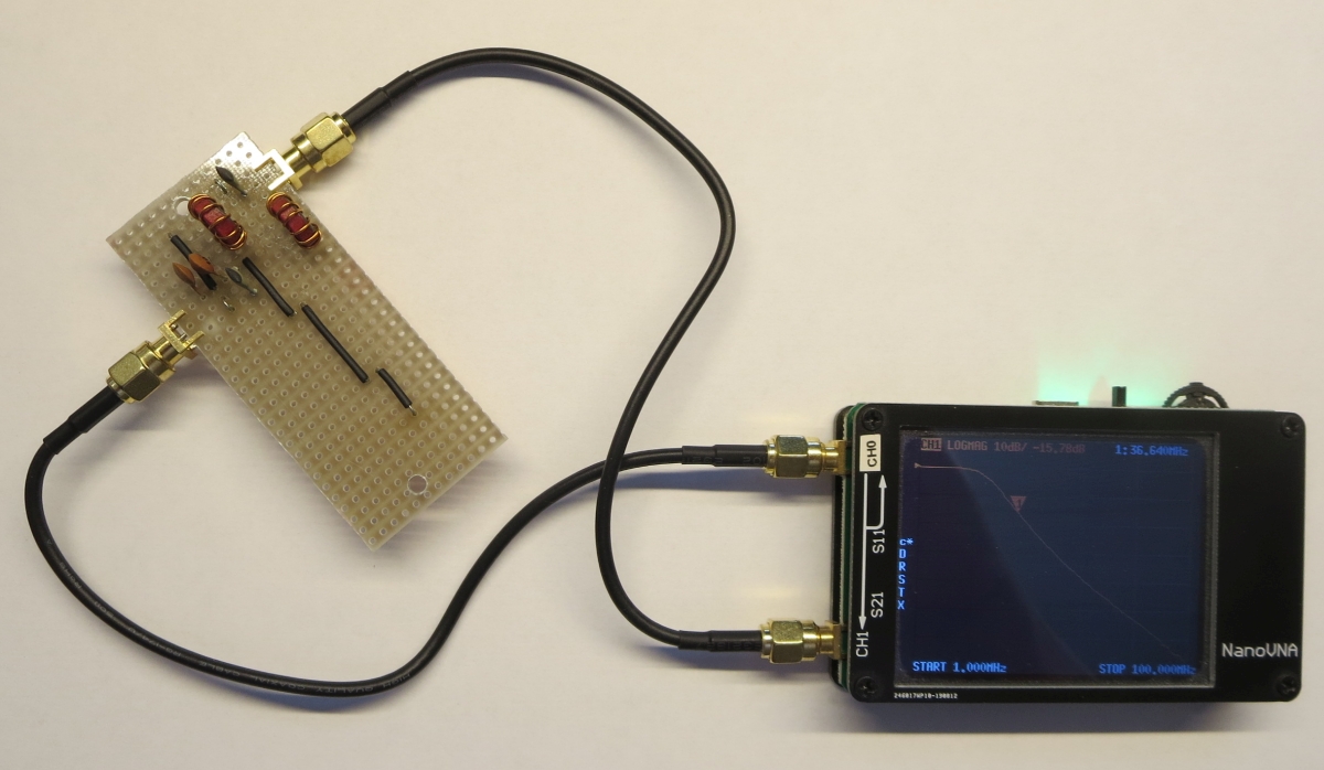
Fig. 12. Measuring the Low Pass Filter. | Measuring the Low Pass Filter
The low pass filter comprises L3, L4, C4, C5, and C6. I measured the frequency response of the filter using NanoVNA.
Start freq: 1 MHz; Stop freq: 100 MHz
Gain at 18 MHz: -0.78 dB
Gain at 36 MHz: -17.7 dB
Gain at 54 MHz: -33.6 dB
Gain at 72 MHz: -47.6 dB
|

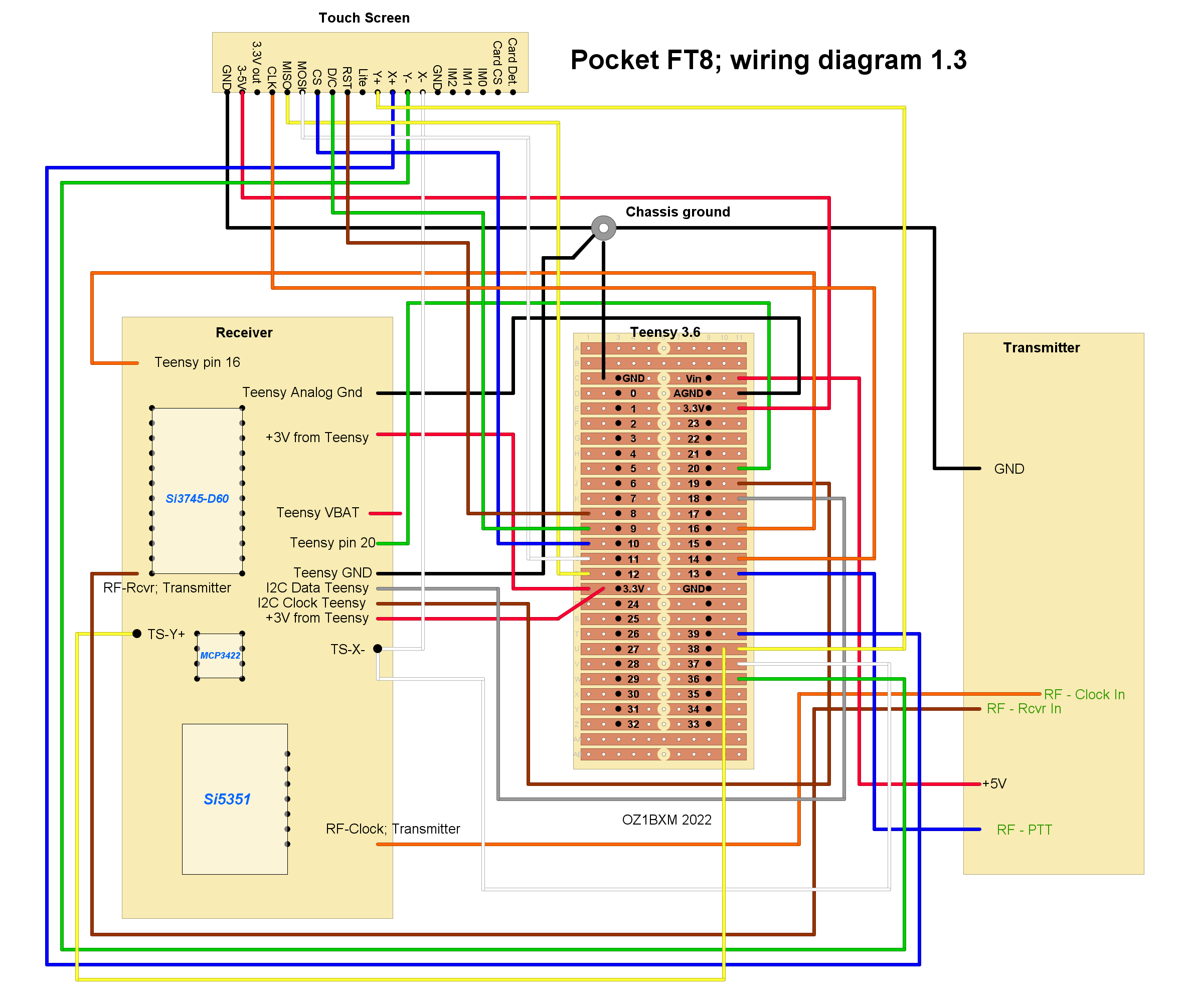
Fig. 13. Wiring diagram (ver. 1.3). | Wiring diagram
The
boards are wired together using insolated wire in different
colors as shown in figure 13. HB9TVK Peter told me, that MISO and
MOSI are reversed in the original diagram in the Project Manual 1.0. MOSI should connect to Teensy pin 11, and MISO to Teensy pin 12.
|
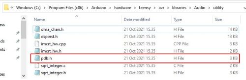
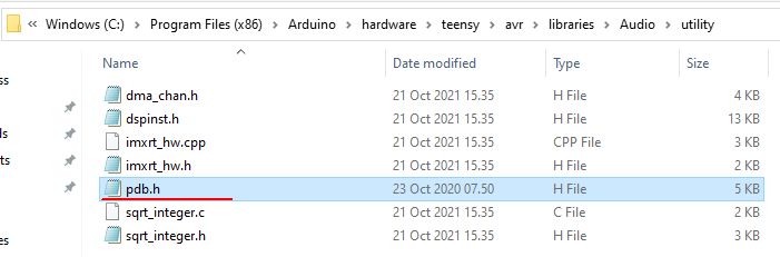
Fig. 14. Pdb.h file. | Load Teensy software into Arduino IDE
Follow the Project Manual page 5 (Building the Firmware).
The instructions https://www.pjrc.com/teensy/td_download.html
will guide you, and soon Teensyduino is installed with a lot
of new libraries. Win 10 advice: Run the installation file as Administrator.
The file
pdb.h in the "utility" folder (high-lighted in figure 14) must be replaced
by the one in the "Pocket_FT8_Publish" folder. |

Fig. 15. The new pdb.h file. | The new pdb.h is shown in figure 15. The new size is 5 kb and the date is 23-Oct-2020. |
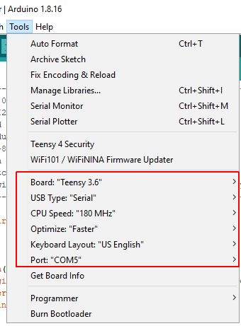
Fig. 16. Teensy 3.6 is detected by Arduino IDE. | Arduino IDE detects Teensy 3.6
Figure 16 shows Arduino IDE > Tools when Teensy 3.6 is connected to the PC and properly detected.
If the Board string is different from "Teensy 3.6", you can select it here:
Tools > Board > Teensyduino > Teensy 3.6 |

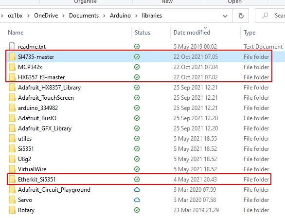
Fig. 17. New libraries. | Install remaining libraries
How to install additional libraries: https://www.arduino.cc/en/guide/libraries
Disconnect Teensy from the PC. Close Arduino IDE and restart the PC. Open Arduino IDE and install the remaining libraries:
- Etherkit_Si5351
- MCP342X
- HX8357_t3-master
- Si4735-master
The new libraries should be installed in the sketchbook folder. Open this folder by selecting:
Arduino IDE > Sketch > Show sketch folder.
Copy the four new library folders to the "libraries" folder inside your sketchbook as shown in figure 17.
Verify that the new libraries are available in the list that pops up when you select Sketch > Include library.
The Etherkit_Si5351 library is displayed as "Etherkit Si5351"
The MCP342X library is displayed as "MCP342x"
The HX8357_t3-master is displayed as "HX8357_t3"
The Si4735-master library is displayed as "PU2CLR SI4735"
The new libraries can also be verified in the Library Manager (select Type = Installed). |
Fig. 18. HX8357_t3.cpp. | Reduce SPI clock speed
HB9TVK
Peter recommends reduce the SPI clock speed from 30 MHz to 25 MHz for
better stability. HB9TVK has experienced erratic display behavior
at 30 MHz. He says the display still works ok at 25 MHz.
Find the HX8357_t3-master folder as shown in figure 18.
Open file HX8357_t3.cpp and go to line 56: #define SPICLOCK 30000000
Change line 56 like this: #define SPICLOCK 25000000 |
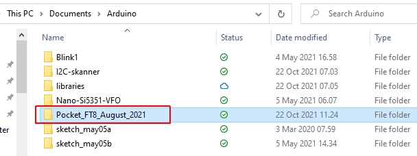
Fig. 19. This folder contains the main software. | Set ham call and locator, compile and upload
Copy the folder "Pocket_FT8_August_2021" to the sketchbook folder as shown in figure 19.
Open the file Pocket_FT8_August_2021.ino and insert your ham call and your locator:
char Station_Call[] = "OZ1BXM"; //six character call sign + /0
char Locator[] = "JO46"; // four character locator + /0
Save the file and press Verify
to compile. Observe, that IDE selects the proper libraries. If
IDE selects a "wrong" library, the "wrong" library must be moved
outside the library folder, or renamed.
Upload the compiled file to Teensy 3.6.
|
| Project status
I have received valuable info regarding the display problem from HB9TVK Peter
The project stopped May 2022. |
|
|
|

